
65nm CMOS Breakthrough: How This Compact Filter Solves the Sub-THz Selectivity Puzzle
We compile, generate and translate using Artificial Intelligence from the below given source. Macro Micro News is responsible for its editorial publication.
Global, Source:
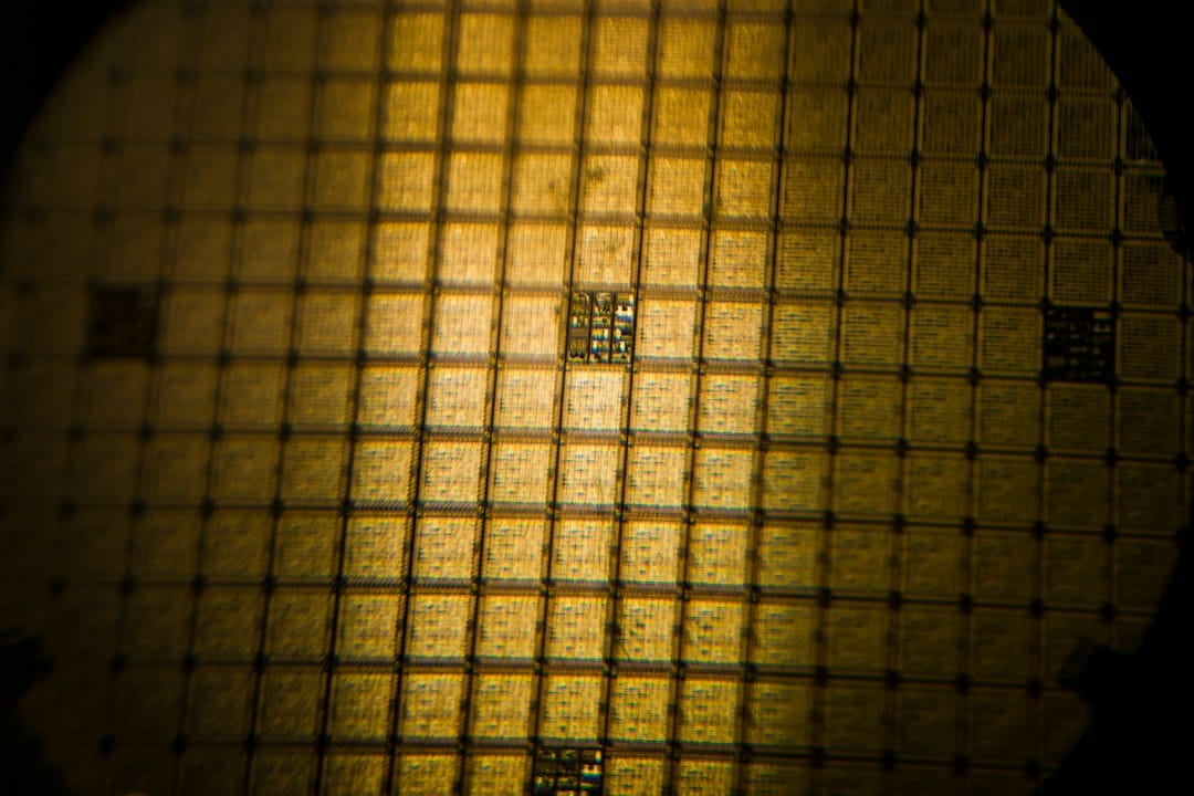
The race for terabit-per-second data rates is pushing wireless systems into the sub-terahertz realm. As spectrum congestion tightens in lower bands, engineers face a physical wall. Traditional passive components simply cannot keep up with the demands of these high frequencies. The solution lies in on-chip integration to eliminate packaging parasitics and boost reliability. Yet, standard CMOS technology struggles here. Lossy silicon substrates and dense metal stacks degrade the quality factors of essential inductors and capacitors. This creates a significant bottleneck for high-speed communication.
Researchers have now introduced a novel bandpass filter designed specifically for 65 nm CMOS technology. This design uses a stub-loaded dual-mode resonator architecture to achieve exceptional frequency selectivity without increasing the circuit area. Conventional methods often rely on complex numerical even-odd-mode analyses. This new approach offers something different. It introduces an LC equivalent-circuit model that provides closed-form pole and zero analysis. This mathematical clarity allows engineers to precisely control transmission zeros. These zeros are critical for sharpening the transition between the passband and stopband.
The core innovation involves a cross-coupled topology that places transmission zeros directly within the initial passband. By reusing the SLR arms for cross-coupling instead of adding dedicated structures, the design reduces the area cost typically associated with high-selectivity filters. The resulting prototype operates at a center frequency of 178 GHz with a fractional bandwidth of 25%. Measured results show an insertion loss of just 5.0 dB. The shape factor reaches an impressive 0.51, indicating a very steep transition from the passband to the stopband.
This filter occupies a minuscule core chip area of 0.129 by 0.273 mm². Normalized to only 0.0124 lambda squared, this compact footprint makes it highly suitable for System-on-Chip platforms. It enables the integration of frequency-division duplexers, image-band suppression in radiometers, and noise reduction in imaging systems. While lumped-element filters struggle above 100 GHz due to degraded capacitor quality factors, and other distributed filters often sacrifice selectivity for size, this design strikes an optimal balance. It outperforms many state-of-the-art CMOS and BiCMOS entries in terms of shape factor while maintaining a competitive absolute area. This advancement marks a significant step forward in making high-speed, high-integrity sub-terahertz communications viable within standard semiconductor manufacturing processes.
Related in Gadgets

Gadgets
How ROI Similarity Solves Point Cloud Noise: A New Standard for Change Detection
Laser point cloud change detection has faced persistent hurdles due to spatial and structural uncertainties. Residual registration errors, uneven point cloud density, viewpoint shifts, and object occlusion frequently lead to false alarms, making accurate monitoring difficult. To…
Read More...
Gadgets
How SMHA Solves the AI Image Quality Puzzle: A New Framework for Precision
The surge in text-to-image generation has reshaped digital creation, yet it brings a pressing question: how do we truly measure the quality of these synthetic visuals? Traditional photos face physical issues like blur or noise, but AI-generated images present a more complex land…
Read More...
Gadgets
How AI Stops Cyberattacks in P2P Energy Markets: Real-Time Detection Explained
The smart grid is undergoing a profound transformation. We are moving away from centralized power plants toward decentralized networks where energy flows bidirectionally. This shift relies on integrating information technology with physical infrastructure. Modern grids now facil…
Read More...
Gadgets
How to Cool EV Motors: The 31% Efficiency Gain in PMSM Design
The push for electric vehicles is accelerating at a rapid pace. This shift brings a significant engineering hurdle to the forefront. Thermal management in permanent magnet synchronous motors has become a critical challenge. Modern drivetrains generate intense heat. This heat con…
Read More...
Gadgets
How AI-Driven RIS on High-Altitude Platforms Boosts Energy Efficiency for IoT
Global, Source In remote rural areas and disaster zones Internet of Things devices often face a frustrating reality weak or blocked connections to terrestrial base stations. This connectivity gap creates significant hurdles for critical applications such as environmental monitor…
Read More...
Gadgets
How Real-Time Iteration NMPC Solves Offshore Wind Turbine Control in Under 5 Milliseconds
Offshore wind turbines equipped with full-power converters face a complex control challenge that requires the simultaneous coordination of power tracking, electrical safety, and mechanical load mitigation. While Nonlinear Model Predictive Control offers a systematic framework fo…
Read More...
Gadgets
How the Nautical δ-Corridor Ensures Safe Autonomous Ship Navigation
The maritime industry stands at a pivotal moment as autonomous surface ships move from experimental phases to regulated commercial deployment. A critical challenge remains: ensuring navigational safety while strictly adhering to international collision regulations. Researchers h…
Read More...
Gadgets
How L1* Regularization Transforms Multi-Modal Anomaly Detection: A New Standard for Semantic Accuracy
In a world where data streams from countless sources, traditional anomaly detection often struggles to keep pace. Most existing algorithms rely on single-modal inputs like text or images alone, missing the intricate correlations that define real-world scenarios. This limitation…
Read More...
Gadgets
How Deep Learning Keeps Remote Solar Security Systems Online
Maintaining uninterrupted surveillance in remote locations presents a unique engineering challenge. Unlike urban infrastructure powered by stable electrical grids, solar-powered security systems rely entirely on intermittent renewable energy sources and finite battery storage. A…
Read More...
Gadgets
How Failure-Guided Control Boosts Au-Wire Bonding Strength by 3x on Silicon Submounts
As programmable photonic integrated circuits expand to support higher port counts and system-level reconfigurability, high-density electrical fan-out has become a critical packaging bottleneck. In the realm of silicon photonics, particularly for devices like optical field-progra…
Read More...