
Class-D Amplifier Limits: Why Switching Frequency Defines Your Audio Fidelity
We compile, generate and translate using Artificial Intelligence from the below given source. Macro Micro News is responsible for its editorial publication.
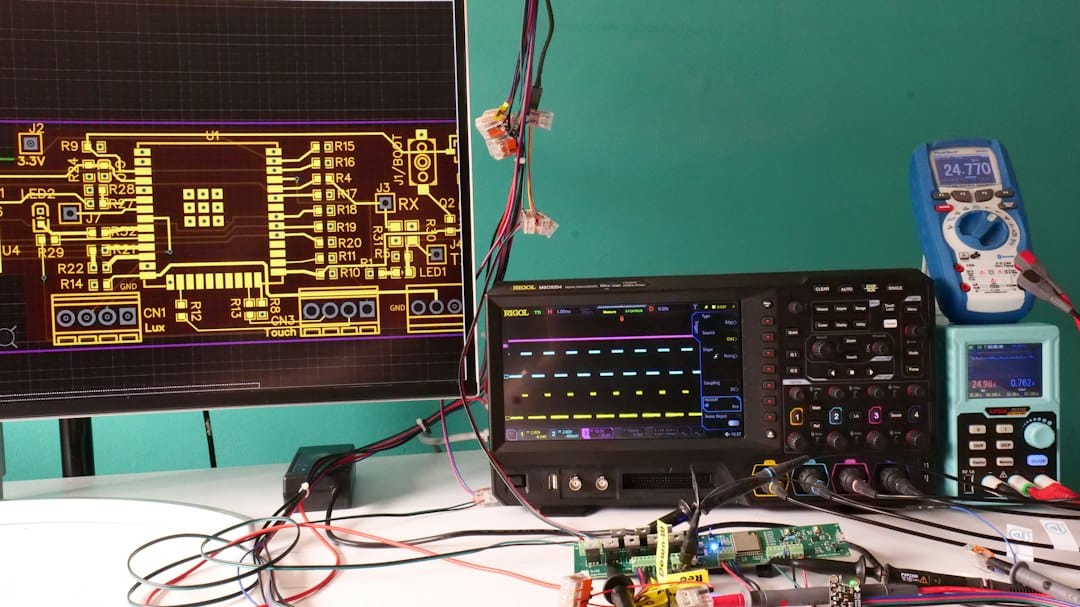
Switzerland, Source:
Class-D amplifiers have long been celebrated for their impressive energy efficiency. Yet achieving pristine audio quality requires navigating a complex web of technical constraints. A recent study in Electronics (MDPI) offers a new framework for selecting the optimal switching frequency in full-bridge Class-D stages. This research suggests that many standard design choices might fall short of high-fidelity standards.
The heart of the challenge lies in pulse-width modulation trade-offs. Raising the carrier frequency lightens the load on the output filter and allows for smaller components. However this increase also boosts switching losses and reduces pulse-width headroom. It further exposes the amplifier to distortion from dead-time intervals. These are brief moments when both switches in a leg remain off to prevent short circuits. The researchers developed closed-form bounds that evaluate reconstruction-filter attenuation, dead-time distortion, pulse-width headroom, and switching loss together. This approach helps designers verify if a specific frequency can meet all requirements before hardware construction begins.
Key findings reveal that a second-order output filter needs a minimum switching frequency of roughly 280 kHz for a standard 20 kHz audio band with 1 dB passband ripple and 40 dB carrier attenuation. Accounting for component tolerances and guard bands pushes this requirement to 347 kHz. At these frequencies the effective blanking interval becomes strictly limited. For example a 2% blanking allocation restricts non-overlap time to just 58 to 71 nanoseconds. Conventional models often overestimate distortion by assuming ideal square-wave commutation. An extended commutation model that includes switch-node charge and inductor ripple proves far more accurate. It aligns with simulations within 7% for blanking intervals above 1%. Traditional formulas can overestimate distortion by up to 51% at 2% blanking.
Semiconductor technology significantly influences performance outcomes. Silicon MOSFETs face tighter limits on switching energy due to reverse-recovery charge constraints. They may struggle to reach high-frequency targets without excessive heat dissipation. Gallium Nitride devices offer faster switching speeds and negligible reverse recovery. This provides a wider feasible operating window. However GaN’s lower output capacitance makes dead-time distortion a dominant factor. Maintaining performance with GaN requires extremely short blanking intervals.
Experimental data from a 14 V amplifier using a 660 ns transition interval highlights the importance of speed. Under derived constraints for high-fidelity audio such a long interval would limit effective bandwidth to about 2 kHz. This renders the design unsuitable for full-range audio applications. Modern high-performance designs therefore utilize nanosecond-level dead times and megahertz-class switching frequencies. The research concludes that joint feasibility analysis is essential. It provides engineers with screening conditions for blanking shortest pulse width and switching energy to ensure robust amplifier designs.
Related in Gadgets

Gadgets
Why Your Browser Says No: The Hidden Logic Behind Access Denied Errors
The digital world moves fast. Yet one experience remains universally frustrating for users everywhere. That sudden stop when a website refuses to load. You see the stark message 'Access Denied' or the HTTP 403 Forbidden code. This is not just a random error. It is a critical sig…
Read More...
Gadgets
Why Your Browser Says No: The Hidden Logic Behind Access Denied Errors
Have you ever stared at a blank screen that simply refuses to let you in? That frustrating 'Access Denied' message is more than just a digital roadblock. It is actually a sign that the internet's security systems are working exactly as they should. When you see an HTTP 403 Forbi…
Read More...
Gadgets
COMBI-CBRN: How Modular Sensors Are Redefining Firefighter Safety in CBRN Emergencies
Global, Source Emergency response teams face a complex puzzle when dealing with Chemical, Biological, Radiological, and Nuclear incidents. The safety of first responders often hinges on the accuracy of initial reconnaissance. Traditional methods frequently rely on separate detec…
Read More...
Gadgets
How Structure-Aware Alignment Boosts AI Accuracy in Partial-Label Learning
The world of artificial intelligence faces a persistent hurdle. Perfectly labeled data is rare and expensive to obtain. Researchers have turned to partial-label learning as a solution. This method allows models to learn from ambiguous supervision. Each instance comes with a set…
Read More...
Gadgets
Boost Weed Detection AI Accuracy Without New Hardware: The MASC Method
Agricultural technology is experiencing a major shift as artificial intelligence models grow more resilient to environmental changes. A new study introduces Metadata-Guided Appearance-Shift Consistency (MASC), a training framework that improves weed detection in outdoor images w…
Read More...
Gadgets
AI Detects Transmission Tower Flaws: 59% Precision Boost for Grid Safety
Modern energy grids depend on the reliability of electrical transmission infrastructure. Manual inspections of towering steel structures remain labor-intensive and prone to human error. A recent breakthrough in computer vision technology offers a transformative solution for iden…
Read More...
Gadgets
How Fault-Aware HIL Verification Secures AUTOSAR Timing Compliance in Modern ECUs
As automotive electronics grow more complex, ensuring the safety integrity of Electronic Control Units (ECUs) has become a top priority under standards like ISO 26262. While functional correctness is routinely validated, timing correctness remains a nuanced challenge. This is es…
Read More...
Gadgets
Why You Are Blocked: The Hidden Mechanics of Web Access Control
Have you ever stared at a screen and seen those three ominous words: Access Denied? It is not just a technical glitch. It is the result of sophisticated security protocols working hard to protect server resources and sensitive data. This phenomenon is a fundamental aspect of how…
Read More...
Gadgets
Why Your Greenhouse Sensors Fail: The MQTT Timing Trap and How to Fix It
Smart greenhouses promise precision agriculture through continuous data streams. Yet many growers face a frustrating reality where wireless sensor networks falter under the weight of their own complexity. A recent study in Electronics (MDPI) sheds light on this issue by introduc…
Read More...
Gadgets
Bit-Accurate FPGA Control: Reliable PV-STATCOM Ride-Through in Weak Grids
As renewable energy integration accelerates, the stability of power grids facing voltage sags and weak grid conditions has become a critical engineering challenge. A recent study published in Electronics (MDPI) addresses this by delivering a comprehensive analysis of bit-accurat…
Read More...